AnandTech Article Channel |

- ZTE to Build Tegra 4 Smartphone, Working on i500 Based Design As Well
- Sony Announces PlayStation 4: PC Hardware Inside
- An Update on Intel's SSD 525 Power Consumption
- Samsung Details Exynos 5 Octa Architecture & Power at ISSCC '13
- Fractal Design Define XL R2 Case Review: Maybe We Can Have It All?
- Intel Demos CloverTrail+ Based Lenovo IdeaPhone K900 Ahead of MWC
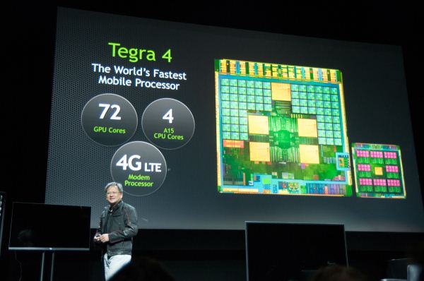
| ZTE to Build Tegra 4 Smartphone, Working on i500 Based Design As Well Posted: 20 Feb 2013 04:00 PM PST
ZTE just announced that it would be building a Tegra 4 based smartphone for the China market in the first half of 2013. Given NVIDIA's recent statements about Tegra 4 shipping to customers in Q2, I would expect that this is going to be very close to the middle of the year. ZTE didn't release any specs other than to say that it's building a Tegra 4 phone. Separately, ZTE and NVIDIA are also working on another phone that uses NVIDIA's i500 LTE baseband.
| ||
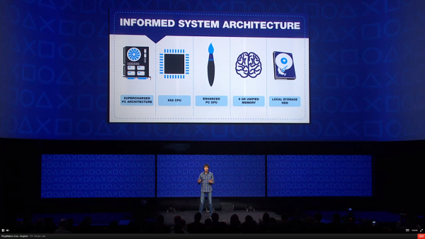
| Sony Announces PlayStation 4: PC Hardware Inside Posted: 20 Feb 2013 02:28 PM PST
Sony just announced the PlayStation 4, along with some high level system specifications. The high level specs are what we've heard for quite some time:
Details of the CPU aren't known at this point (8-cores could imply a Piledriver derived architecture, or 8 smaller Jaguar cores - the latter being more likely), but either way this will be a big step forward over the PowerPC based general purpose cores on Cell from the previous generation. I wouldn't be too put off by the lack of Intel silicon here, it's still a lot faster than what we had before and at this level price matters more than peak performance. The Intel performance advantage would have to be much larger to dramatically impact console performance. If we're talking about Jaguar cores, then there's a bigger concern long term from a single threaded performance standpoint. Update: I've confirmed that there are 8 Jaguar based AMD CPU cores inside the PS4's APU. The CPU + GPU are on a single die. Jaguar will still likely have better performance than the PS3/Xbox 360's PowerPC cores, and it'll should be faster than anything ARM based out today, but there's not huge headroom going forward. While I'm happier with Sony's (and MS') CPU selection this time around, I always hoped someone would take CPU performance in a console a bit more seriously. Given the choice between spending transistors on the CPU vs. GPU, I understand that the GPU wins every time in a console - I'm just always an advocate for wanting more of both. I realized I never wrote up a piece on AMD's Jaguar architecture, so I'll likely be doing that in the not too distant future. The choice of 8 cores is somewhat unique. Jaguar's default compute unit is a quad-core machine with a large shared L2 cache, it's likely that AMD placed two of these together for the PlayStation 4. The last generation of consoles saw a march towards heavily threaded machines, so it's no surprise that AMD/Sony want to continue the trend here. Clock speed is unknown, but Jaguar was good for a mild increase over its predecessor Bobcat. Given the large monolithic die, AMD and Sony may not have wanted to push frequency as high as possible in order to keep yields up and power down. While I still expect CPU performance to move forward in this generation of consoles, I was reminded of the fact that the PowerPC cores in the previous generation ran at very high frequencies. The IPC gains afforded by Jaguar have to be significant in order to make up for what will likely be a lower clock speed. Backwards compatibility with PS3 games isn't guaranteed and instead will leverage cloud gaming to stream older content to the box. There's some sort of a dedicated background processor that handles uploads and downloads, and even handles updates in the background while the system is off. The PS4 also supports instant suspend/resume. We don't know specifics of the GPU, but with approaching 2 TFLOPS we're looking at a level of performance somewhere between a Radeon HD 7850 and 7870. Update: Sony has confirmed the actual performance of the PlayStation 4's GPU as 1.84 TFLOPS. Sony claims the GPU features 18 compute units, which if this is GCN based we'd be looking at 1152 SPs and 72 texture units. It's unclear how custom the GPU is however, so we'll have to wait for additional information to really know for sure. The highest end PC GPUs are already faster than this, but the PS4's GPU is a lot faster than the PS3's RSX which was derived from NVIDIA's G70 architecture (used in the GeForce 7800 GTX, for example). I'm quite pleased with the promised level of GPU performance with the PS4. There are obvious power and cost constraints that would keep AMD/Sony from going even higher here, but this should be a good leap forward from current gen consoles. Outfitting the PS4 with 8GB of RAM will be great for developers, and using high-speed GDDR5 will help ensure the GPU isn't bandwidth starved. Sony promised around 176GB/s of memory bandwidth for the PS4. Leveraging Gaikai's cloud gaming technology, the PS4 will be able to act as a game server and stream the video output to a PS Vita, wirelessly. This sounds a lot like what NVIDIA is doing with Project Shield and your NVIDIA powered gaming PC. Sony referenced dedicated video encode/decode hardware that allows you to instantaneously record and share screenshots/video of gameplay. I suspect this same hardware is used in streaming your game to a PS Vita. The lack of solid state storage isn't surprising. Hard drives still offer a dramatic advantage in cost per GB vs. an SSD. Now if it's user replaceable with an SSD that would be a nice compromise. The new box heavily leverages PC hardware, which is something we're expecting from the next Xbox as well. It's interesting that this is effectively how Microsoft entered the console space back in 2001 with the original Xbox, and now both Sony and MS have returned to that philosophy with their next gen consoles in 2013. The PlayStation 4 will be available this holiday season. I'm trying to get more details on the CPU and GPU architectures and will update as soon as I have more info.
| ||
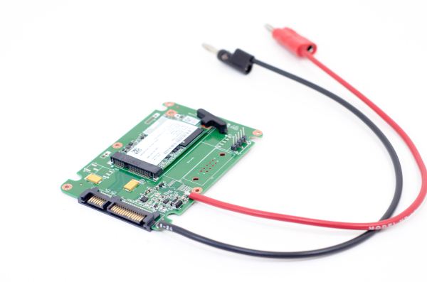
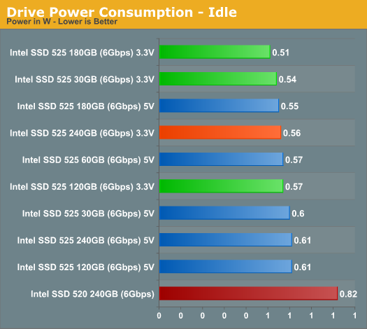
| An Update on Intel's SSD 525 Power Consumption Posted: 20 Feb 2013 11:55 AM PST
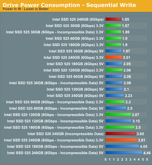
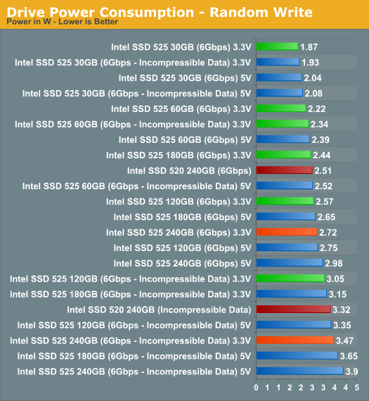
Intel's SSD 525 is the mSATA version of last year's SF-2281 based Intel SSD 520. The drive isn't just physically smaller, but it also features a new version of the Intel/SandForce firmware with a bunch of bug fixes as well as some performance and power improvements. Among the improvements is a tangible reduction in idle power consumption. However in our testing we noticed higher power consumption than the 520 under load. Intel hadn't seen this internally, so we went to work investigating why there was a discrepancy. The SATA power connector can supply power to a drive on a combination of one or more power rails: 3.3V, 5V or 12V. Almost all 2.5" desktop SSDs draw power on the 5V rail exclusively, so our power testing involves using a current meter inline with the 5V rail. The mSATA to SATA adapter we use converts 5V to 3.3V for use by the mSATA drive, however some power is lost in the process. In order to truly characterize the 525's power we had to supply 3.3V directly to the drive and measure at our power source. The modified mSATA adapter above allowed us to do just that. Idle power consumption didn't change much: Note that the 525 still holds a tremendous advantage over the 2.5" 520 in idle power consumption. Given the Ultrabook/SFF PC/NUC target for the 525, driving idle power even lower makes sense. Under load there's a somewhat more appreciable difference in power when we measure directly off of a 3.3V supply to the 525: Our 520 still manages to be lower power than the 525, however it's entirely possible that we simply had a better yielding NAND + controller combination back then. There's about a 10 - 15% reduction in power compared to measuring the 525 at the mSATA adapter's 5V rail with the 240GB model. There story isn't any different in our random write test. Measuring power sent direct to the 525 narrows the gap between it and our old 520 sample. Our original 520 still seems to hold a small active power advantage over our 525 samples, but with only an early sample to compare to it's impossible to say if the same would be true for a newer/different drive. I've updated Bench to include the latest power results.
| ||
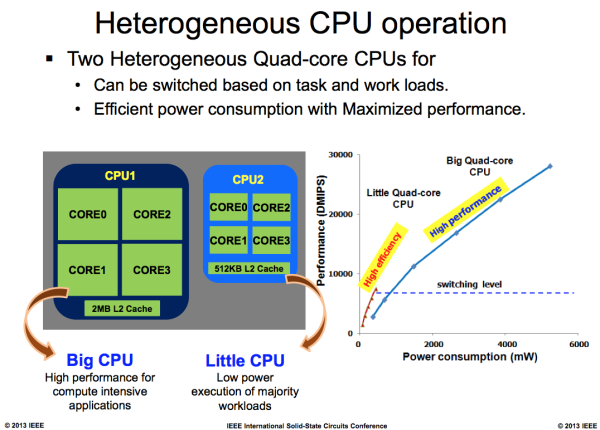
| Samsung Details Exynos 5 Octa Architecture & Power at ISSCC '13 Posted: 20 Feb 2013 08:42 AM PST
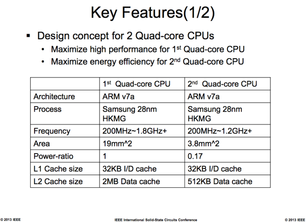
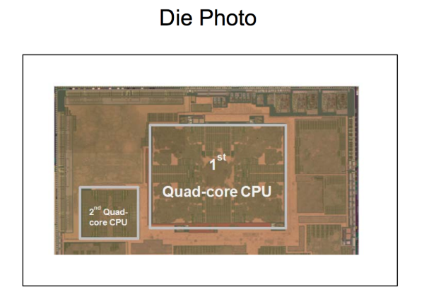
At CES this year Samsung introduced the oddly named Exynos 5 Octa SoC, one of the first Cortex A15 SoCs to implement ARM's big.LITTLE architecture. Widely expected to be used in the upcoming Galaxy S 4, the Exynos 5 Octa integrates 4 ARM Cortex A7 cores and 4 ARM Cortex A15 cores on a single 28nm LP HK+MG die made at Samsung's own foundry. As we later discovered, the Exynos 5 Octa abandons ARM's Mali GPU for Imagination's PowerVR SGX 544MP3, which should give it GPU performance somewhere between an iPad 3 and iPad 4. The quad-core A7 can run at between 200MHz and 1.2GHz, while the quad-core A15 can run at a range of 200MHz to 1.8GHz. Each core can be power gated independently. The idea is that most workloads will run on the quad-core A7, with your OS hot plugging additional cores as performance demands increase. After a certain point however, the platform will power down the A7s and start switching over to the A15s. Both SoCs implement the same revision of the ARM ISA, enabling seamless switching between cores. While it's possible for you to use both in parallel, initial software implementations will likely just allow you to run on the A7 or A15 clusters and switch based on performance requirements. What's most interesting about Samsung's ISSCC presentation is we finally have some hard power and area data comparing the Cortex A15 to the Cortex A7. The table above puts it into numbers. The quad-core A15 cluster occupies 5x the area of the quad-core A7 cluster, and consumes nearly 6x the power in the worst case scenario. The area difference is artificially inflated by the fact that the A15 cluster has an L2 cache that's 4x the size of the A7 cluster, but looking at the die photo below you can get a good feel for just how much bigger the A15 cores are themselves: In its ISSCC presentation, Samsung stressed the value of its custom libraries, timing tweaks and process technology selection in bringing the Exynos 5 Octa to market. Samsung is definitely marching towards being a real player in the SoC space and not just another ARM licensee. The chart below is one of the most interesting, it shows the relationship between small integer code performance and power consumption on the Cortex A7 and A15 clusters. Before switching from the little CPU to the big one, power consumption is actually quite reasonable - south of 1W and what you'd expect for a smartphone or low power tablet SoC. At the lower end of the performance curve for the big CPU things aren't too bad either, but once you start ramping up clock speed and core count power scales linearly. Based on this graph, it looks like it takes more than 3x the power to get 2x the performance of the A7 cluster using the Cortex A15s.
| ||
| Fractal Design Define XL R2 Case Review: Maybe We Can Have It All? Posted: 20 Feb 2013 08:01 AM PST Amusingly and appropriately enough, the wave of silence-oriented enclosures that have been popping up recently haven't really drawn attention to themselves as a trend. Yet all of a sudden, we have results from a couple of solid contenders from Nanoxia and a few less expensive (and more readily available) also-rans. For a little while, this was a wave that Fractal Design was riding high, but the Define R4 wound up being a little underwhelming. As it turns out, they might just have something better lying in wait. We never had a chance to play with the original Fractal Design Define XL, so it's tough to draw a direct comparison there. Yet one look at Fractal Design's page for the original tells you that while the Define R4 didn't change much from the R3, the Define XL R2 is a major shift. The original XL didn't support E-ATX; it was more just a conventional Define with a separate drive compartment. This R2, on the other hand, really is a giant Define R4. As it turns out, that bump in size and modest increase in cooling capacity may very well have been all the Define R4 needed.
| ||
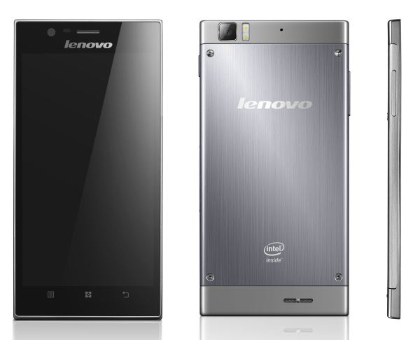
| Intel Demos CloverTrail+ Based Lenovo IdeaPhone K900 Ahead of MWC Posted: 20 Feb 2013 07:59 AM PST
Lenovo announced its ultra slim (6.9mm) 5.5" 1080p IdeaPhone K900 at CES earlier this year, based on Intel's presently unannounced CloverTrail+ SoC. While we're expecting to learn a lot more about CT+ next week at MWC, Intel did post a video showcasing the K900's performance. The video below includes footage of the K900 running Epic's Citadel for Android very smoothly at 1080p, as well as PR TextureMark. PR TextureMark is a video decode/GPU texturing/memory bandwidth benchmark, although Intel was careful not to actually run the benchmark on the phone. Intel's Atom SoCs have always been very good on the memory interface side compared to the ARM competition, which makes PR TextureMark an obvious showcase for the platform. Epic's Citadel runs well on the K900, but as we showed earlier, it runs well on just about every high-end Android smartphone at this point. It's clear that the CT+ based K900 however integrates a much better GPU than the PowerVR SGX 540 included in Medfield, as the latter wouldn't be able to run Citadel at 1080p this smoothly. I should also point out that some have been incorrectly assuming that the K900 is based on Intel's forthcoming Merrifield silicon. Merrifield and the rest of Intel's 22nm SoC lineup isn't due to ship/sample until the latter part of this year. Lenovo's K900 will be available in China starting in April, and expanding to other territories afterwards.
|


.jpg)
| You are subscribed to email updates from AnandTech To stop receiving these emails, you may unsubscribe now. | Email delivery powered by Google |
| Google Inc., 20 West Kinzie, Chicago IL USA 60610 | |


No comments:
Post a Comment