AnandTech Article Channel |

| Posted: 18 Nov 2012 04:07 PM PST
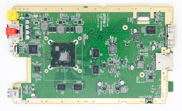
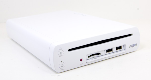
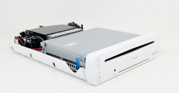
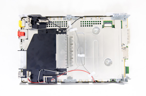
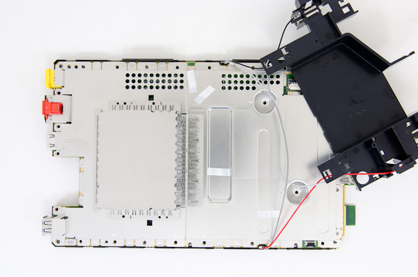
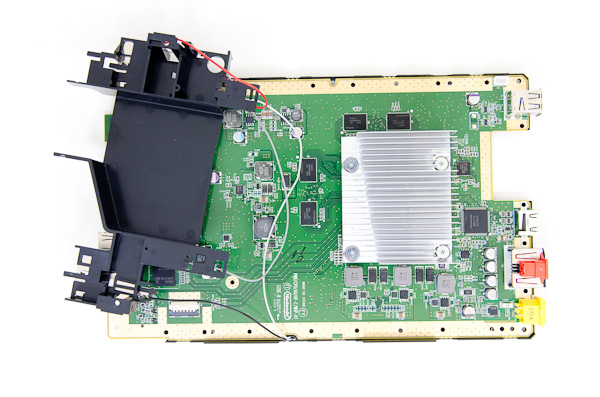
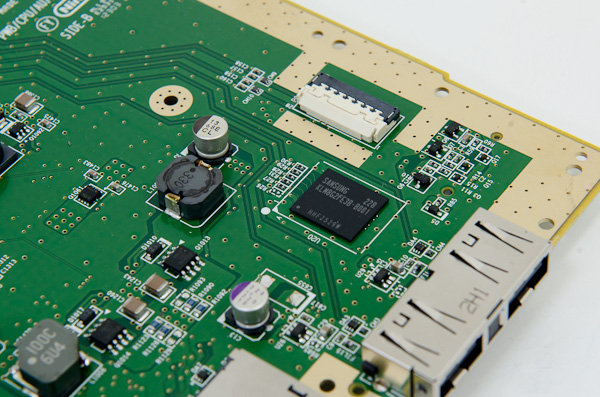
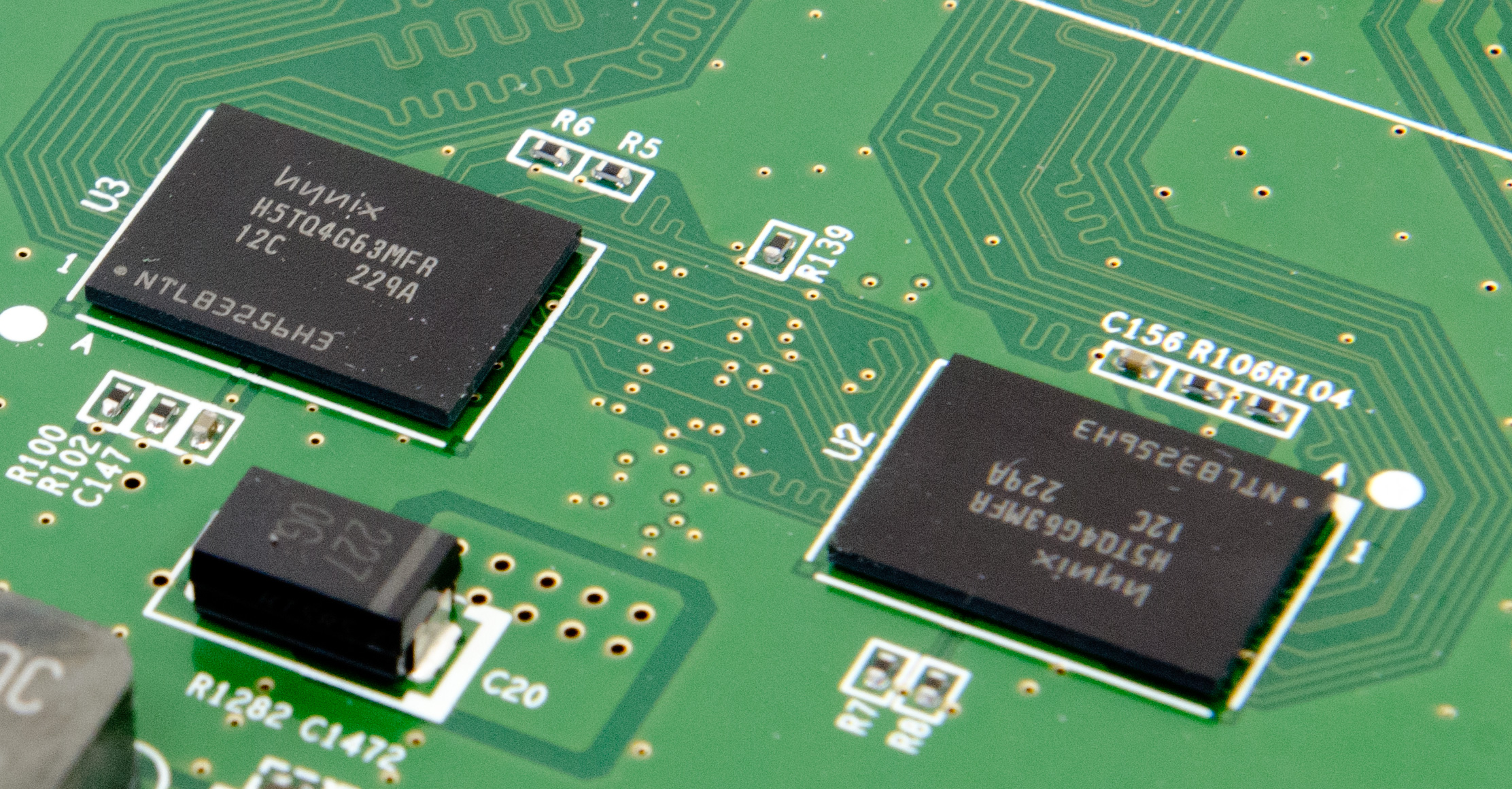
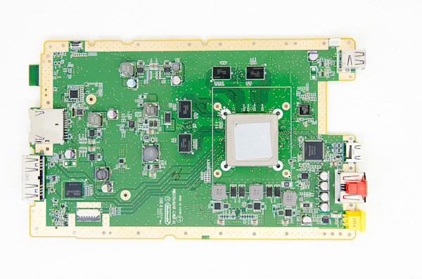
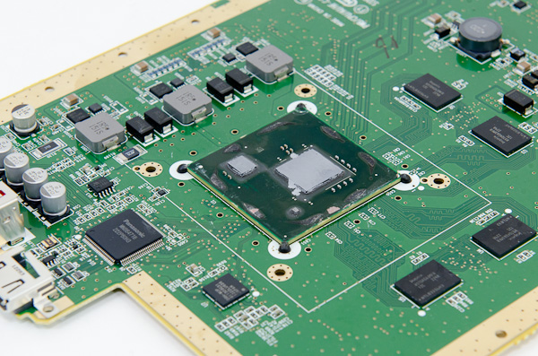
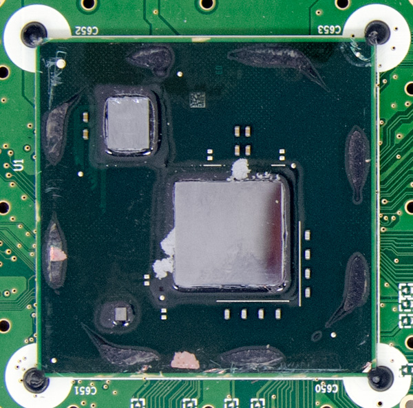
When Nintendo announced the Wii U there was a lot of interest in its hardware specs. The new console could very well end up the fastest kid on the block thanks to the sheer age of the Xbox 360 and PlayStation 3. I wasn't all that interested in the Wii U, but I did want to get a look at the silicon inside so I grabbed a unit and went into teardown mode. The Wii U is available in two versions: the basic and deluxe kits. The basic kit comes in white, while the deluxe is black. Both are glossy. The deluxe console gives you 32GB of on-board storage (eMMC NAND) vs. 8GB for the standard model. The deluxe kit also includes a stand and cradle for the Wii U The Wii U hardware itself looks a lot like a larger Wii. Getting inside the chassis is also quite similar. The CMOS battery door is the first thing you'll have to remove, followed by 8 more screws (a mixture of philips head and tri-wing). The bulk of these screws are behind console-colored stickers, be sure to peel them all off. With all 8 (9 including the CMOS battery door) screws removed, you can slide the left side of the Wii U away from the front of the console, and off all together. This reveals the final three tri-wing screws that you'll need to remove to get inside the chassis (the gallery of all of this is at the bottom of the article). With all 12 screws removed, pry the top of the Wii U up and away from the body until it separates from the rest of the frame revealing the console's fairly compact internals: The Wii U optical drive uses a custom format for game storage, but offers a very Blu-ray-like 25GB capacity per disc. Max sequential read speeds are pretty high compared to the current gen consoles at 22MB/s. Two screws hold the front cover in place, followed by four screws that hold the optical drive in place. Be careful when removing the optical drive as there's a ribbon cable attached to the motherboard for power/data. The same goes for the front cover, although its ribbon cable is really only on light/switch duty. With the optical drive removed, next up is removing the shielding on the top and bottom of the motherboard and the shround on top of the heatsink. Just go around the perimeter of the motherboard removing screws (you'll be able to remove all but two easily). Once you've done this, the motherboard will be able to separate from the Wii U's lower tray. Removing the shielding itself requires carefully moving the antenna cables out of the way. As these wires are soldered to the Wii U chassis on one end, be very careful not to pull too hard otherwise you run the risk of needing to break out the soldering iron. If you've removed all of the screws and freed the antenna wires from their guides a bit, you should be able to pull back the plastic heatsink shroud, revealing...more shielding: With no screws left to hold it in place however, the shielding is easily dealt with (again pay close attention to the antenna wires). The same is true for the bottom of the PCB. The two sets of antenna wires go to two independent wireless controllers: one for 802.11b/g/n WiFi, the other to a dedicated 802.11n controller to handle Miracast display streaming between the Wii U and the GamePad display. Thanks to Ryan Shrout over at PC Per for figuring this one out! Once you've removed all shielding you're left with a pretty clean looking motherboard: On the top side of the board you'll see the eMMC/NAND package, in this case it's a dual-die Samsung eMMC solution (there's another Toshiba NAND device on the back of the board, not for user storage): There are four 4Gb (512MB) Hynix DDR3-1600 devices surrounding the Wii U's MCM (Multi Chip Module). Memory is shared between the CPU and GPU, and if I'm decoding the DRAM part numbers correctly it looks like these are 16-bit devices giving the Wii U a total of 12.8GB/s of peak memory bandwidth. (Corrected from earlier, I decoded the Hynix part numbers incorrectly). Our own Ryan Smith found a great reference for the original Wii so we can compare memory frequencies. It looks like the original Wii had a 32-bit wide GDDR3 memory interface running at a max datarate of 1.4GHz for a total of 5.6GB/s of bandwidth (excluding eDRAM). That doesn't sound like a lot (it's the same amount of memory bandwidth on the Nexus 10 and iPad 3/4), but the Wii U is supposed to have a good amount of eDRAM for both the CPU and GPU to use. Also keep in mind that the Nexus 10 and iPad 3/4 have to drive much higher resolutions than the Wii U does. The Wii U's MCM is unfortunately covered by a heatspreader, but given that I went through all of this to look at the console's silicon, I was going to look at the console's silicon. Normally to remove an integrated heat spreader (IHS) you grab a sharp blade and go around cutting the (hopefully) glue around the perimeter of the chip. In the case of the Wii U's MCM, the blades I'd normally use were too thick. A few years ago I decided to give shaving with a double edge safety razor a try. My attempts failed poorly, but I had a stack of unused DE razor blades that were thin enough to get the IHS off. The trick here is to apply enough pressure to the blade to cut through the glue, as simply trying to saw through the glue will take forever. There are two blobs of glue per side, but if you're trying to remove the IHS be careful not to cut through the glue and scrape any of the actual exposed silicon...like I did. With the IHS off, we have the Wii U's MCM in all of its glory: There are actually three components on this single package, made in at least two different microprocessor fabs. The multicore PowerPC based CPU is the smaller of the two larger chips. This die is made on IBM's 45nm SOI process. The RV7xx derived GPU is the biggest die on the package, and I'm presuming it was made on a 40nm process. I'm assuming the very tiny die in the corner is actually some off-chip memory. Both the CPU and GPU in the Wii U are supposed to have some eDRAM, although the bulk of it is likely dedicated for the GPU. The approximate die sizes for all components on the MCM are in the table below:
If we assume a 40nm process for the GPU, then we're looking at something a bit larger than the RV740. The Wii U does boast backwards compatibility with games made for the original Wii, which is made possible thanks to a shared ISA with the original PowerPC based Wii. The size comparison between CPU and GPU die shouldn't be too much of a surprise. When building a dedicated gaming machine it always makes sense to throw more transistors at your GPU. The nearly 5x ratio of GPU to CPU die size here is a bit on the extreme side though. I suspect many of the current generation consoles, including the Wii U, suffered from a lack of a powerful yet affordable CPU solution that could be easily implemented.
Gallery: Nintendo Wii U Teardown       I also took some power measurements on the Wii U. The system is powered by a 75W external power supply, but total system power consumption doesn't even hit half of that (at least with the games I tried):
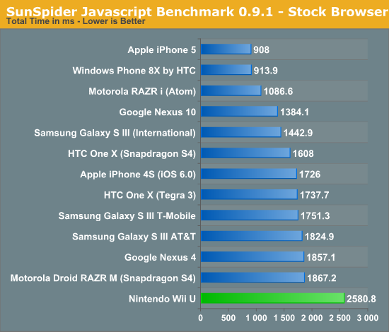
Rendering the Wii U menu actually consumes almost as much power as playing Super Mario U. Watching a movie on Netflix consumes a bit less power, my guess is a lot of the 3D blocks are power gated leaving only the CPU cores and video decode hardware active. The Wii U ships with its own web browser based on webkit, the user agent string for the latest version of the Wii U's software is: Mozilla/5.0 (Nintendo WiiU) AppleWebKit/534.52 (KHTML, like Gecko) NX/2.1.0.8.21 NintendoBrowser/1.0.0.7494.US. Pages load quickly and compatibility is surprisingly decent (HTML5 test: 258 + 4 bonus points). By default you control and view the browser on the GamePad, but you can also choose to display the content on your TV via the console. Scrolling is very smooth and the overall experience is way better than what you'd normally expect from a web browser on what's primarily a game console. It's not quite as good as using a modern tablet, but still usable. And where there is a browser, we will run SunSpider on it: The browser is using an older version of WebKit, which is likely responsible for some of the not absolutely stellar performance here.
| ||||||||||||||||||||||||||||||||||||


| You are subscribed to email updates from AnandTech To stop receiving these emails, you may unsubscribe now. | Email delivery powered by Google |
| Google Inc., 20 West Kinzie, Chicago IL USA 60610 | |


No comments:
Post a Comment